Structural and electrical characterization of 2D gradient layers
Description
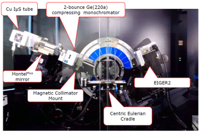
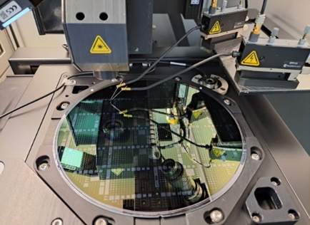
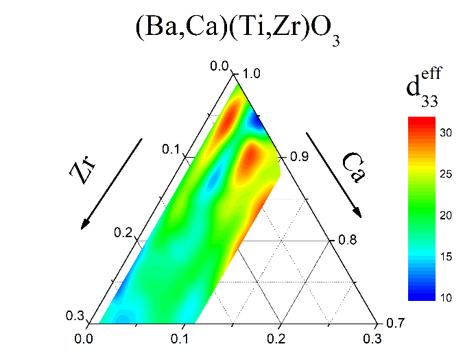
A pool of local and high throughput characterization techniques to evaluate combinatorial heterostructures at the wafer level has been set-up. The local structure is investigated by x-ray micro-diffraction with X,Y automation allowing data collection on a combinatorial library overnight. To characterize the local ferro/piezo/die/electric properties, discrete top electrodes are micro-fabricated (100×100 mm2) to complete capacitive heterostructures with a continuous bottom electrode. Automated probe stations equipped with ferroelectric testers, Dual Beam Laser Interferometer or Impedance meter allows measurements of hundreds of capacitors in a few hours. Automated data treatment produce maps of ferroelectric (Ps, Hc), piezoelectric (d33) and dielectric (e, tand) versus position.
Location
Laboratory GREMAN, UMR-7347 CNRS-University of Tours
Technical characteristics
Micro-diffractometer Bruker D8 Discovery
- Thin film diffractometer
- Micro-source with parallel/parallel beam + 2 and 4 reflection monochromator
- 300 µm collimator
- Detector 2, θ-2θ,
- Texture, RSM, reflectometry
- Grazing incidence and in-plane diffraction
- Variable temperature 100 K-1200 K


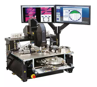
Probe-station A
- Electrical characterization of structures in vertical or coplanar topology, depending on position on the sample, using automated sub-tip stations (1×1cm² sample to 6″ wafer), temperature-controlled (-55°C to 150°C)
- Generic impedance characterization as a function of frequency (100 Hz to 10 MHz), with optional DC voltage ± 40 V, leakage current up to ± 200 V
- Ferroelectric-specific characterizations (P(E),C(VAC) up to ± 10 V)
Probe-station B
- AIXACCT Dual Beam Laser Interferometer
- Position-dependent characterization of piezoelectric materials using automated sub-tip stations: P(E), displacement, PUND, up to ± 200 V
- Reflective top and bottom surfaces required

Associated targeted project
